Analog Devices ADAR4002 - A Digitally Programmable Delay Circuit For RF Applications

Programmed delays and attenuation are helpful in a variety of RF scenarios. The ADAR4002 from Analog Devices is an attenuation IC that operates from 500 MHz to 19 GHz.
Signals are sent to the ADAR4002 via its RF1 port and are then attenuated and time-delayed, as shown in the block diagram.
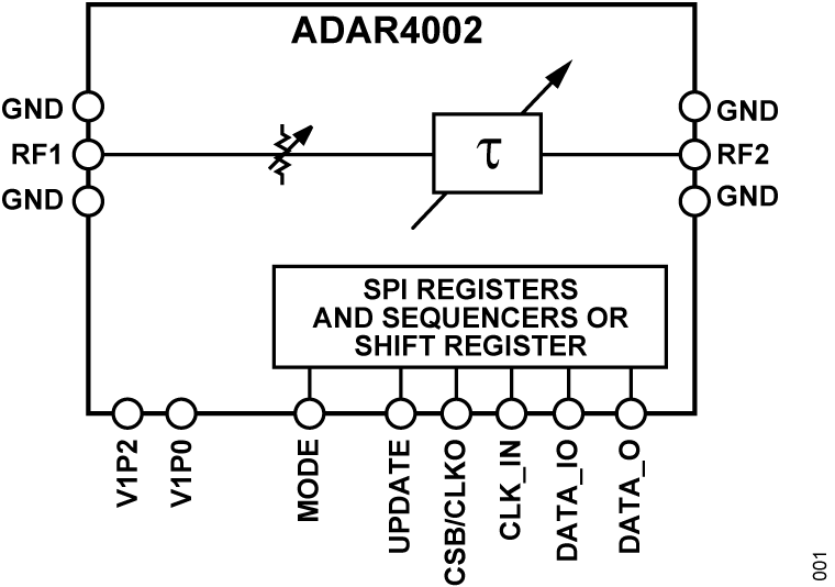
The bottom of the chart reveals the presence of an SPI transmitter, which can be used to modify the behavior of the attenuator and the delay element. This way, the ADAR4002 becomes a flexible, universal tool for a wide range of signal path conditioning tasks. For example, varying delays caused by A/D or PCB design constraints can be compensated for with digital settings. Furthermore, these parameters can be stored off-chip, thereby greatly simplifying the calibration of the RF path.
2ps Resolution for Accurate Timing
One classic application of the chip is phase correlation: signals are strategically delayed to ensure they arrive at a specific point on the printed circuit board without phase shift.
The chip\'s seven-bit time-delay unit can operate in two modes. Range zero has a broader range and is intended for lower-frequency signals, while range one can handle faster signals thanks to its higher time-slot accuracy. In particular, the data sheet provides the following information about the available ranges:
Range 0: 0 ps to 508 ps with 4 ps standard resolution
Range 1: 0 ps to 254 ps with 2 ps high resolution
Integrated Attenuator for Leveling Applications
RF signal path design is greatly simplified if a signal can be assumed to have the correct level. For the ADAR4002, Analog Devices provides a DSA unit that serves a function similar to a fine-granular programmable attenuator.
It can be programmed via the chip\'s SPI interface and allows the designer to add attenuation to the signal passing through the digital delay line. In the data sheet, the following specifications are given for its RF performance:
The DSA has 6-bit resolution with an attenuation range of 0 dB to 31.5 dB and a step size of 0.5 dB
Shift Register and SPI Modes for Flexible Programming.
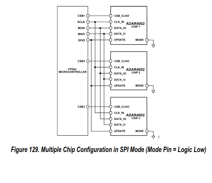
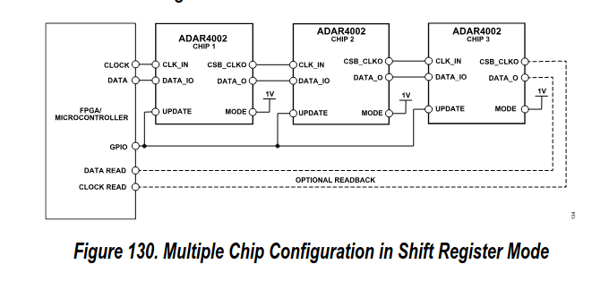
RF parameters enter the chip via its digital interface. For this, Analog Devices provides two operating modes. If the mode pin is held at logic low, the system implements a classic SPI interface that a variety of application microcontrollers can drive. If the mode pin is held high, the ADAR4002 operates in shift register mode.
The reason for this duplication is that ADAR4002 chips can be chained, allowing a single digital interface to set multiple RF attenuator behaviors. In SPI mode, one control line is required per chip, as shown in the figure below.
In shift register mode, components can be connected directly to one another.
Power Management
Thanks to its highly efficient internal design, the ADAR4002 can be driven with a supply voltage of only 1.2 V. If higher voltages are required, current will be sunk, as shown in the figure below.
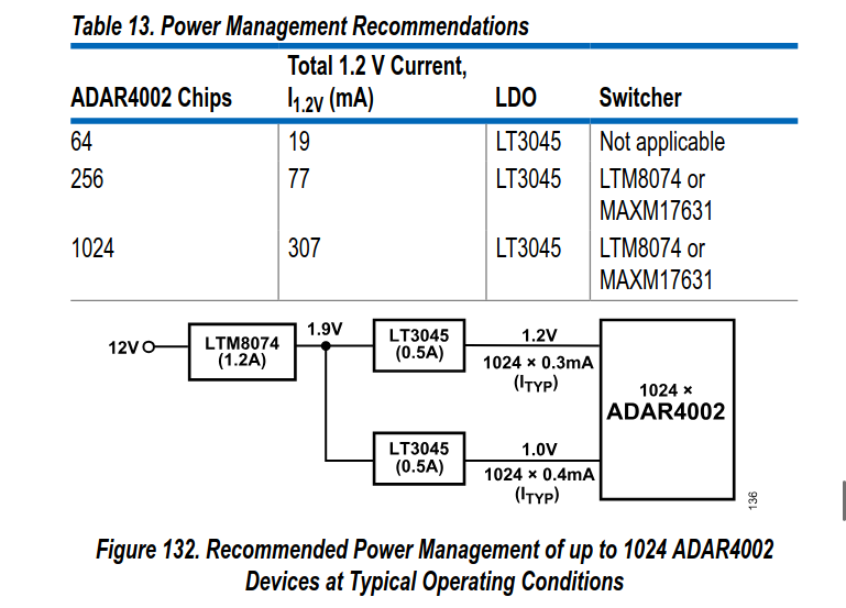
The data sheet provides recommendations for complex power chains. For this, regulators such as the LT3045 are to be used as shown.
Conclusion
If a phased array radar or a similar RF application requires high-performance phase correlation for fast signals, the ADAR4002 is an excellent choice. Thanks to the highly flexible attenuation settings, the ease of programming, and the low power consumption, RF designers can solve a variety of tasks with a single chip. In short, a component that is always deserving of recommendation.